

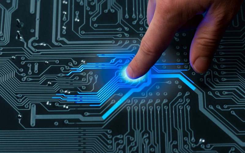
In electronics, printed circuit boards or PCBs are the fundamental component that allow most devices and systems in the modern world to function. find its usage in everyday use device like mobile phones, laptops, computers, home automation systems, automobiles, and even complex applications such as in industrial automation, and even medical equipment. However, with the latest advancements in device structures and the increasing operating frequencies of new technologies, signal integrity has become a crucial factor that has to be addressed when designing and developing a hardware board or when selecting appropriate hardware engineering solutions.
Signal integrity is defined as the aspects of signal quality where signals retain properties such as waveform and timing at the output end which is same as that at its input end. Low signal quality can result in a range of problems for the system and its components such as data error, electromagnetic interference and even the outright failure of the system. Thus, signal integrity refers to the design strategy employed when producing PCBs with the aim of improving electrical performance and assuring the device’s functionality.
Understanding Signal Integrity Challenges
The issues surrounding signal integrity can be ascribed to various elements such as high operating clock frequencies, complex manufacturing designs, intricate signal routing, the use of multilayer boards, and fast rising data rates. When signals go through the hierarchy of PCB traces, vias, and connectors, they are vulnerable to a number of adversities, including signal reflections, coupling, ground noise, and attenuation.
Reflections and Impedance Mismatch
If a signal interacts with an impedance discontinuity or faced impedance mismatch in its path , part of the signal gets reflected back to the source distorting the signal and in certain situation maybe lead to complete signal integrity problem. These reflections may happen at via transitions, connector interfaces or at anyplace a line width changes drastically.
Crosstalk
This is an effect that happens as a result of signals that are found on two consecutive planes or tracks in a PCB interfering with each other through electromagnetic interlinkage. This is not an ideal scenario and can result in signal interference, and sometimes data corruption or failure to meet timing specifications. When there are two or more parallel traces carrying high-density signals in close distances, crosstalk is always a menace.
Ground Bounce and Power Integrity
Switching noise is commonly referred to as ground bounce which is a disturbance that transmits simultaneously through the ground plane when several output drivers switch at once in a circuit. This can cause voltage oscillations on the ground reference where Analog and digital circuits meet, causing signal degradation and logical failures.
Signal Attenuation and Dispersion
While PCB traces and connectors conduct signals, both space and frequency domain characteristics may be affected by attenuation and dispersion. Attenuation results to reduction in signal amplitude in proportion to signal length and frequency while dispersion results in signal delay and get worst at higher frequency or longer trace length.
Designing for Signal Integrity
These identified signal integrity challenges indicate that electrical performance issues in the signal path must be adequately addressed through key design techniques and hardware engineering solutions in the context of hardware board design. These are issues oflayout, control of impedance, power plane and power distribution grid design, and the design of complex simulation models and simulation tools.
Power Distribution Network Optimization
To recap, a good PDN is therefore important for providing reference voltages both for power and ground; they are associated with signal integrity. Some of the important guidelines in the design of the PDN include the correct selection and positioning of decoupling capacitor, especially the low impedance power planes and proper POF current carrying capacities. Other more sophisticated methods, now available and recognized in the design process, include power plane segmentation and embedded capacitance to improve power integrity.
Advanced Simulation and Verification
Today, for instance, new material and geometrical hardware engineering solutions rely on commercial state-of-art, as well as simulation and verification tools, to study and improve signal integrity at the design phase. Some of the benefits that can be achieved by using electromagnetic or EM simulation tools include ability to look for or observe problems likely to occur between the traces, via and connector and, come up with possible solutions in advance.
These tools can simulate each design variable at a very detailed level, including crosstalk, reflections, and losses, and enable the engineers to make critical adjustments to the designs before making drastic changes by investing in physical prototyping.
High-Speed Serial Interfaces
HSSIs the abbreviate of High-Speed Serial Interface, which plays crucial role in the contemporary common sense communication protocol comprehending the USB, PCI Express and Ethernet. It is important to preserve signal integrity in these interfaces, because any small distortion can result in page data damage and more transmissions errors. techniques such as equalization, pre-emphasis and de-emphasis can be used to ameliorate attenuation as well as distortions commonly associated with signals.
Original Field and System-on-Chip (SoC) Integration
The methods of designing embedded hardware and system on chip designs are quite different hence signal integrity can be a big problem. Many of these are called System on Package (SOP), which currently contain digital, analog, and radio-frequency (RF) elements, which are closely interconnected and mean that an effective separation and protection has to be designed due to crosstalk and noise issues.
Conclusion
Managing signal integrity on PCB stands as an important niche in the field of hardware board design as well as a part of hardware engineering solutions necessary to improve the electrical characteristic and overall functionality of PCBs. Through analysis of SI problems, use of appropriate design strategies, application of powerful computer-aided tools and applications, and adherence to various standards, designing PCBs for operating in the harsh environment of today’s electronics is achievable.
This is important especially as technology advances and with signal integrity as one of the important factors that is enhanced, the call for design methodologies, materials, and tools will foster greater advancements. Thus, with a continuous focus on these advancements, hardware engineering professionals can rest assured that their designs would be in parity with the contemporary demands and standards of the electronics industry.